|
January 2009
Advancing Research at the Smallest Level: GW’s New Institute for Nanotechnology
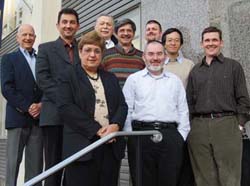
Faculty members collaborating on nanotechnology research include (back row, left to right) David Nagel, Edward Della Torre, and Jason Zara; (middle row, left to right) Can Korman, Jon Silver, and Yongsheng Leng; and (front row, left to right) Mona Zaghloul, Michael Keidar, and Ryan Vallance.
|
By Julia Parmley
Imagine moving, manipulating, and researching materials a billion times smaller than a meter. Sixteen faculty members in the Columbian College of Arts and Sciences and the School of Engineering and Applied Science are doing just that in the newly created GW Institute for Nanotechnology (GWIN).
“Nanotechnology is a vital area of national importance with applications across a wide spectrum, from medicine to electronics to improving water quality worldwide,” says David Dolling, dean of GW’s School of Engineering and Applied Science and professor of mechanical and aerospace engineering. “National laboratories, federal agencies, and private sector corporations all recognize the as-yet untapped potential for discoveries in this emerging field, and we believe that our engineers and scientists will be among those who unlock some of its exciting secrets.”
The institute is supported through special endowment funding designated for academic programs with the potential for a high level of intellectual distinction. Funding was allocated in the fall after a request made last year by Executive Vice President for Academic Affairs Donald R. Lehman for research proposals from faculty elicited multiple submissions for nanotechnology research. The research involves manipulating natural and man-made materials with dimensions less than 100 nanometers. Eight hundred 100-nanometer particles placed side by side is equal to the width of a human hair.
Led by Professor of Mechanical Engineering Ryan Vallance, the institute brings together faculty from mechanical and aerospace engineering, electrical and computer engineering, civil and environmental engineering, physics, chemistry, and biochemistry.
The researchers are examining nanostructured materials and their properties, applications and devices incorporating nanostructures, computational modeling and analysis, and nanomanufacturing and metrology. Projects underway include developing a system for nanopatterning with scanning tunneling microscopy, studying growth of carbon nanotubes, computational mechanical modeling of nanomaterials, researching nanomagnetics, and filtration with nanostructured materials.
According to Dr. Vallance, the field of nanotechnology has blossomed in the past few decades spurred by scientific advancements, the semiconductor industry, and new instrumentation, including the scanning electron tunneling microscope and the atomic force microscope, which can measure nanostructures with atomic resolution.
“Nanotechnology holds great promise for a wide variety of fields, including mechanics, electronics, energy, the environment, and health care,” says Dr. Vallance. “There is also a need for research to study the possible dangers of nanotechnologies.”
Dr. Vallance says GWIN researchers hope to establish a new microscopy facility with state-of-the-art instruments for faculty and student use and to forge partnerships with the National Institutes of Health, the National Institute of Standards and Technologies, and the Naval Research Laboratory.
“We have also begun a series of seminars that bring experts in specific nanotechnology areas to campus, and Professor Jon Silver has begun a journal club in which faculty and students read and discuss exciting new publications in nanotechnology,” says Dr. Vallance. “We want to develop new knowledge in the field as well as educate students about how to research and use nanotechnology.”
GWIN collaborator and Assistant Professor of Mechanical and Aerospace Engineering Michael Keidar is researching the plasma physics and chemistry behind carbon nanotubes, nanostructures that have potential applications for electronics, optics, and bioengineering. Dr. Keidar and his researchers have already developed microscopic plasma jets that can potentially target individual biological cells and reduce tissue damage during laser surgery.
“GWIN will be a great forum for combining research forces to work on new ideas,” says Dr. Keidar, adding that GWIN will also provide new research opportunities and courses for students.
“Nanotechnology calls for an extremely diverse approach, and we have a breadth and depth of experts who can gather in a common interest to explore its possibilities,” says Peg Barratt, dean of Columbian College and professor of psychology. “The institute will build our knowledge about matter on an atomic and molecular scale, and our professors will share that science-based analysis with students and with the world.”
Send feedback to: bygeorge@gwu.edu
|
|

|